Welcome to the fascinating world of PCB design! Whether you're an electronics enthusiast, a budding engineer, or a seasoned professional, this blog is your gateway to unlock the secrets of successful PCB design.
Starting a new hardware project can be overwhelming, but the completely overhauled Copilot simplifies the process by guiding you through component selection, spec verification. Just describe your goals and Copilot engages in a focused conversation to refine your requirements like a seasoned hardware engineer.
Get help defining your project requirements, block diagram, and research components
Ask me a structured set of questions (about 5 one at a time) to help brainstorm and outline the most important parts of a project including the critical technical requirements, including power, components, performance, constraints, Use case etc
Always provide multiple options where applicable, considering trade-offs in cost, efficiency, size, and performance. By the end of this process, I want:
1. A block diagram illustrating the system architecture.
2. A complete list of all components, including passives and active components.
Go from a block diagram to specific components in a BOM
Here's a block diagram of this design. Please recommend at least three ICs from the @library for each block, highlighting their electrical characteristics and the reasons for your recommendations.
Streamline Parts Research
Instead of wading through datasheets and Google searches, use Copilot to select appropriate parts for implementation, recommending main and alternative components that meet design requirements. Tip: You can use tool like @library to direct Copilot to search the part library, or @file to direct Copilot to use datasheet details in it’s responses.
Get a list of part recommendations based on your requirements
@library List out 5 switching regulators that I can use for my project with a maximum output current of 2A. Include key parameters such as input voltage range, output voltage range, switching frequency, efficiency, and package type.
Identify alternative components for @U4 with similar functionality, pin configurations, and electrical characteristics. Include key differences and trade-offs.
@file Explain @U1 in detail, including its purpose, key functions, and common applications. Describe how it operates within a circuit and any notable characteristics. Also, explain the family or series this component belongs to, highlighting its variations, key differences, and typical use cases compared to other models in the series.
@file Extract the recommended operating conditions for @IC2. Retrieve key parameters such as supply voltage range, operating temperature range, input/output voltage levels, and other relevant conditions specified for optimal performance.
Compare LMR33630ADDAR and MP2451DJ-LF-Z in terms of efficiency, output ripple, load regulation, and thermal performance. Highlight key differences in topology, switching frequency, and suitability for a [specific application, e.g., battery-powered wearable]. Provide a recommendation based on [input voltage range, output voltage, current requirements.
Analyze all the parts in the project context and generate a consolidated parts table that optimizes component selection. Specifically, apply the following consolidation rule:
- Identify passive components (resistors, capacitors, inductors) with the same values but different MPNs (Manufacturer Part Numbers).
- Propose a single standardized MPN for each unique value, prioritizing parts with better availability, and popular supplier.
Present the table clearly. The table must strictly list and analyze all passive components in the project context. It must not use vague terms such as “etc.” or truncate the list in any way. The table should have the following headers (Original Part Category (e.g., Resistor, Capacitor, Inductor), Original Values/Specs (e.g., 10kΩ, 1μF, 100mH), Original MPNs (List all variants found in the project), Proposed Consolidated MPN (Recommended single part), Reason for Consolidation (e.g., same specs, better tolerance, reduced part diversity)
Edit Projects with Copilot
Copilot isn’t just here to answer questions—it can take direct action in your project, helping you place components, modify properties, and refine your design faster than ever. Instead of manually searching for parts or tweaking values one by one, you can ask Copilot to handle specific tasks, like adding a resistor with a defined value or updating a component’s footprint.
When Copilot detects an action it can execute, you’ll see an action button appear—click it to apply the change instantly. If you don’t see a button, try rephrasing your request or breaking it into smaller steps. While Copilot can’t yet generate an entire schematic at once, it’s great at guiding you through the process, handling tedious tasks, and keeping your workflow smooth.
When working on a design, precise calculations are key—but instead of crunching numbers manually, Copilot can help streamline the process. Whether you need to size a resistor, calculate power consumption, or verify signal integrity, you can use Copilot to gather equations and relevant data before running calculations.
Start by pulling in the necessary formulas and values using @file or @library, ensuring you have all the details upfront. Once you’ve gathered the required inputs, use the @calculator tool to perform the calculations accurately. Taking this structured approach will help you get the most reliable results from Copilot.
Using IPC standards calculate ... (e.g., trace width)
@calculator calculate the required PCB trace width for the 12V power rail according to the IPC-2221 standard. The trace should handle a current of 3A with a maximum allowable temperature rise of 10°C. Assume a copper thickness of 1oz and an ambient temperature of 25°C.
@copilot, use mermaid-formatted block diagrams to generate 2 well-detailed architecture design of this project for comparison. Make sure to use the technical and functional requirements information.
@copilot, I’m designing a custom voice-controlled speaker and I initially want it to have buttons, Bluetooth, Wi-Fi, and rechargeable battery. Help me brainstorm and develop a comprehensive product requirements document. Ask me one question at a time, waiting for my response before moving to the next question.
@copilot, validate the the suggested architecture in the block diagram matches the product requirements set for this project. Point out any missing blocks that would be needed to satisfy the requirements.
Design Circuit Blocks
Brainstorm and optimize modular circuit blocks for faster hardware development.
@copilot, here's the block diagram of this design. In a table format, recommend at least 3 IC for each block highlighting the electrical characteristics of the IC and why you recommended it.
Minimum set of components to implement the typical circuit
@copilot, list all components specified in the datasheet of U1 for building the typical application circuit. Present the information in a detailed table format with equations needed to size the components.
@copilot, outline the electrical characteristics of U4 as detailed in the datasheet. Then, suggest at least four drop-in replacement parts, presented in a table format with the columns
@copilot, query all components in the schematic that do not have an assigned manufacturer part number (MPN). Compile these components into a table format with the following details: Designator, Component Function, Electrical Properties, and Recommended MPN (Provide a list of recommended part numbers based on the component's properties, focusing on the most popular and widely available parts).
Improve Supply Chain
Focuses on optimizing component selection and management, including consolidating similar passive components and addressing part obsolescence to streamline the bill of materials and reduce costs.
@copilot, perform a BoM consolidation review to identify passive components (resistors, capacitors, and inductors) that have similar but different values (within ±50%) and the same package code. The goal is to simplify the BoM and reduce costs by replacing these components with a single value where possible, without affecting the circuit's functionality.
For each group of similar components, compare their electrical and mechanical characteristics, then identify a single value that can replace the others. Provide a detailed comparison table for each group, listing the designators, component values, package codes, and the proposed consolidated value, along with key specifications and any additional notes. Document the final proposed consolidated BoM in a table format.
@copilot, identify all components in the schematic that are either obsolete or not recommended for new designs (NRND). Compile these components into a table with the following details: Designator, Description/Function, Obsolete/NRND Status, Recommended Alternative Parts (Suggest at least 2 alternative components and their MPN that are current, widely available, and suitable replacements, based on the original component's specifications).
Calculate Component Values
Involves precise calculations for sizing various components often using Python for accuracy and presenting results in detailed tables.
@copilot, use the datasheets of LED D5 and D2 to obtain electrical characteristics needed to calculate the appropriate current-limiting resistor value. Then use python to calculate the value and present it in a well detailed table forma.
Research Components
Involves detailed examination of integrated components to ensure proper component selection and usage in the design.
@copilot, from the datasheet of U2 List the pin names, functions, and additional attributes for the IC. Include the following details for each pin in a table format: Pin Name, Function, Pin Type (e.g., power, ground, signal), Pin Direction (e.g., input, output, bidirectional, passive), Default State (e.g., high, low, floating), Voltage Level (if applicable), Additional Notes (e.g., pull-up/pull-down resistor, special considerations).
@copilot What are the absolute maximum ratings for U5? Identify any critical components that must be carefully selected to stay within these limits and present the results in a well detailed table format.
Data Visualization and Analysis
Utilizes Python to create visual representations of design data to assist in analysis and decision-making.
@copilot, list all ICs and the decoupling capacitors attached to each. Ensure to include all ICs present in the design, including digital ICs, power converters, LDOs, etc. For every IC, clearly state:
What power net the decoupling capacitors are attached to. What is the stated voltage of that net.
The voltage rating and value of the attached decoupling capacitors.
Signal with the expression “[WARNING]” if any of the following conditions are met: no decoupling capacitors are attached; the voltage of the power net is higher than the voltage rating of the capacitor; No voltage range was stated for the capacitor. Give a separate “[WARNING]” for each condition. Signal with the expression “[OK]” if none of those conditions are met
@copilot, review the design to ensure all current-limiting resistors for LEDs are correctly calculated for a current range of 1mA to 10mA. Follow these steps:
Identify all LEDs and their resistors.
Reference the datasheets for forward voltage (Vf) and current (If). Make no assumptions in this step
Calculate the correct resistor values.
Verify that schematic values match calculations.
Document findings in a table with LED designator, Vf, If, calculated resistor value, schematic value, status, and notes.
Calculates and analyzes the efficiency of PMIC in varying load conditions
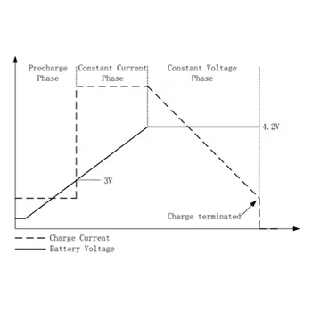
@copilot, determine the efficiency of U4 at various load conditions, considering that the input is a battery with a voltage range from 4.2V (fully charged) to 3.3V (low battery level). Identify which components in the circuit affect this efficiency and present that in a detailed table. Finally, use python to plot a graph showing the efficiency of U1 across the range of load conditions and input voltages.
Testing and Reliability Analysis
Generates test plans and collaborative workflows, ensuring your hardware is manufactured error-free.
@copilot, develop an FMEA (Failure Mode and Effects Analysis) report in a table format that analyzes the systems schematic, each unique component specification, and operational parameters. It should identify critical failure modes, assess their impact, and recommend mitigation actions based on severity, occurrence probability, and detectability. Include columns such as: process step, potential failure mode, potential failure effect, S, O, D, RPN, Action Recommended, and any other you see fit.
Initial Brainstorming
Copilot can help get you started quickly by understanding the requirements and providing guidance.
@copilot I'd like to build a smart curtain that opens or closes based on the amount of sunshine I want to enter my room. How would you approach designing this? Please ask me questions to help with the development.
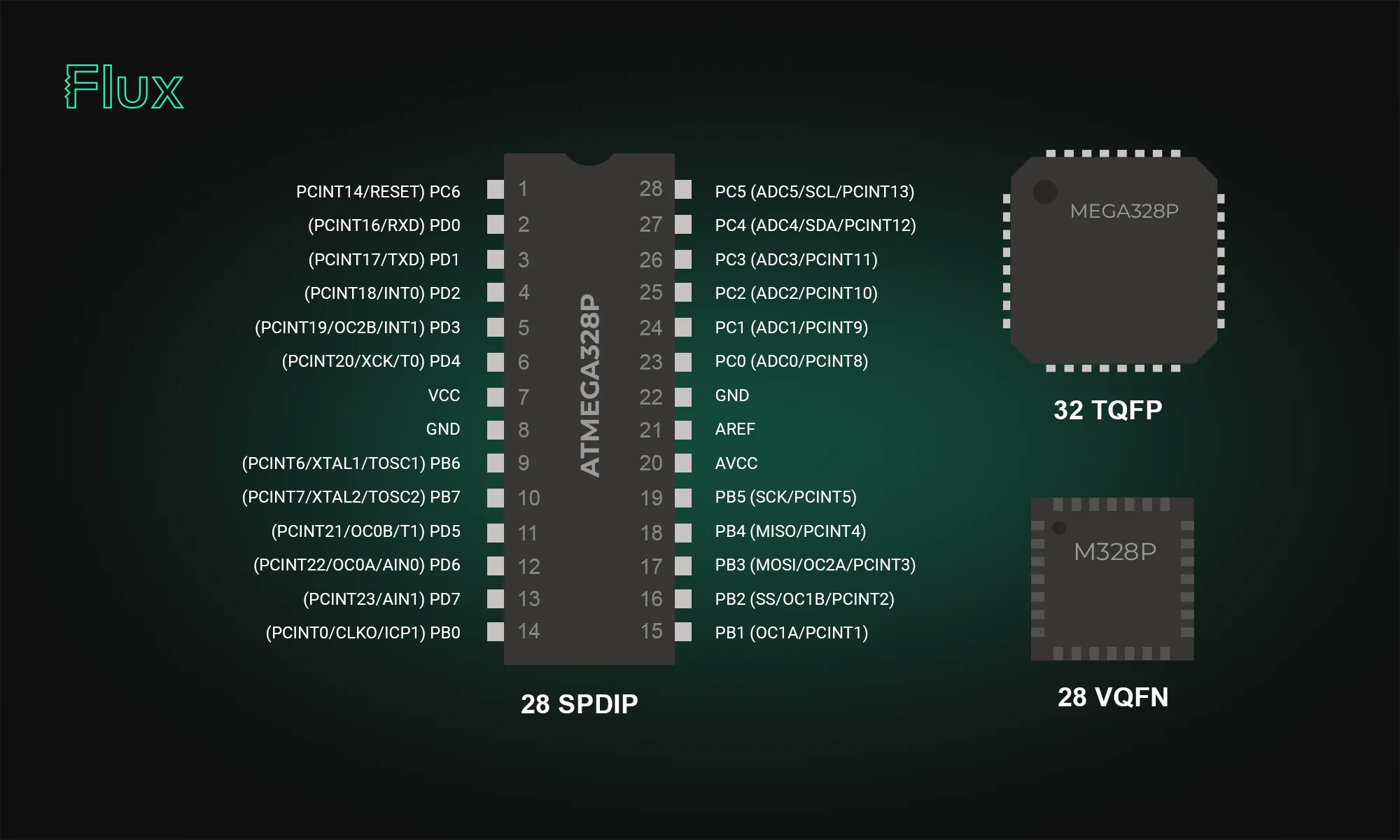
@copilot can you choose 4 digital pins on the ATMega328P-AU that I have here to use as GPIO given that I am already using some pins for reset, the external clock, UART, and I2C.
Combing Through Huge Datasheets
Copilot can understand datasheets and reference them in its responses. This means you get more accurate responses when asking Copilot questions about specific parts.
Copilot answers questions about how to use Flux by referencing our documentation. So, instead of getting stuck and searching documentation, you can stay in the flow and get the help you need without leaving your project!
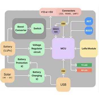
@copilot I want to build a PCB that uses a solar panel to charge a single cell LiPo battery. I want to measure ambient pressure with a microcontroller and send that over WiFi. What are all the components I would need?
Find Alternate Parts
Copilot can offer tailored suggestions and analyze tradeoffs based on your project goals, constraints, and specifications.
@copilot are there any alternatives to U2 that have better availability?
✨ Pro Tip: Use @tools to give Copilot more direction
Flux Copilot has a range of tools to help you through your design process. For the best results, use one tool at a time. This helps Copilot focus on a single task, making its responses more accurate and actionable.
Use @library to direct Copilot to search Flux’s library of components. This is useful when you want to insert components that are in the parts library.
Use @file when you want to direct Copilot to access datasheets, PDFs, or other documents that are attached to your project or components when conducting detailed analysis. You can also attach files to the prompt itself.
Use @calculator when you want Copilot to calculate a value with deterministic instead of relying solely on AI reasoning.
Use @code to create Python code snippets to create graphs, simulate, or validate design ideas.
Use @help to get guidance on using Flux features and best practices.
Flux Copilot is here to make hardware design more straightforward and efficient. By following these prompts and tips, you can streamline your workflow, reduce errors, and tackle each step of your project with confidence. Feel free to share your results and favorite prompts in our Slack Community.
Design a low-noise microphone preamplifier for an electret condenser mic feeding a 24-bit ADC. You must calculate the bias network, gain-setting resistors, coupling capacitors, input high-pass cutoff, output anti-aliasing RC, and decoupling layout. Follow the op-amp and microphone capsule datasheets, ADC input requirements, and industry best practices. It will be integrated into a design. Supply: 3.3V analog rail. Mic bias: 2.0 V through resistor, current ~0.5 mA. Target gain: 20 dB to 40 dB switchable. Bandwidth: 20 Hz to 20 kHz. Input noise target: as low as practical. Include pop-suppression considerations and star-grounding strategy.
No items found.
No items found.
No items found.
Throughout this article, I’ll also share with you various strategies and tips for surpassing the obstacles in your path. In today's digital age, where electronic devices have become an integral part of our lives, understanding the intricacies of PCB design is crucial for anyone seeking to create innovative and reliable electronic products.
What is PCB Design?
PCB, short for Printed Circuit Board, is the backbone of virtually every electronic device we encounter today. Your iPhone has multiple of it, your laptop, your noise-cancelling headphones, your big flat tv, your smart watch, everything that are battery-powered devices for sure have one or more inside. PCB is a flat board made of non-conductive material, often fiberglass, with a layer of copper on one or both sides. The copper traces on a PCB act as electrical pathways, connecting various electronic components such as resistors, capacitors, inductors and complicated integrated circuits, and enabling them to work in harmony.
It is the critical bridge between the abstract world of circuitry and the tangible reality of electronic devices. Well-designed PCBs ensure the optimal performance, functionality, and reliability of electronic products. Whether it's a smartphone, a medical device, or a space exploration module, a thoughtfully designed PCB is the key to unlocking the full potential of the underlying electronics.
Factors to Consider in PCB Design
Electrical Performance
So, what factors should one consider before stepping into the fascinating world of printed circuit board design? While there are numerous aspects to keep in mind, let's highlight a few crucial ones. First and foremost, electrical performance takes center stage. The PCB design must account for signal integrity, power distribution, and electromagnetic compatibility, to prevent issues like signal degradation, voltage fluctuations, and unwanted interference.
A pcb layout ensuring compatibility with its 3D printed enclosure's size and shape.
Mechanical Considerations
But it doesn't end there. Mechanical aspects also play a vital role in PCB design. The size, shape, and mechanical support of the PCB are crucial factors in ensuring compatibility with the intended enclosure or system. Heat dissipation, component placement, and routing efficiency are all critical in preventing thermal issues and maintaining overall system reliability.
Manufacturability and Cost
Manufacturability and cost-effectiveness should never be overlooked. Designing a PCB that should be easily fabricated, assembled (does it needs hot-air solder or just solder iron), and tested without compromising quality is essential for efficient production. Considering factors such as the vias spec, trace width and spacing, choice of dielectric materials, cores, component sourcing, and production techniques can significantly impact the overall cost and time-to-market of the final product.
PCB Design Requirements
Which PCB Design Software Should I Use?
When it comes to PCB design, the software or EDA/CAD you choose plays a vital role in the success of your design process. It can greatly impact the efficiency, accuracy, and overall quality of your final PCB layout. One EDA software that stands out in this regard is flux.ai. It offers a range of innovative features, including a community part library, a hardware AI assistant, and automated impedance control, making it a top contender worth considering.
What sets flux.ai apart is its integration of a hardware AI assistant, Flux Copilot. This advanced feature utilizes artificial intelligence to provide intelligent recommendations and guidance throughout your design journey. It's like having a knowledgeable companion by your side, helping you make informed decisions, optimize your designs, and minimize the chances of errors.
Another impressive feature of flux.ai is its latest feature: automated impedance control. This is particularly important in high-speed designs where maintaining signal integrity is crucial. By automating the impedance control process, flux.ai simplifies the task of achieving precise impedance matching. You just have to look for a component in the community library, add it to the schematic editor, and wire the pins together; then if the system detects you're using a component that needs impedance control - flux.ai will take care of the rest for you. This saves valuable time and effort for designers, allowing them to focus on other critical aspects of their design.
When selecting PCB design software, it's essential to consider your specific design requirements, ease of use, available features, and compatibility with your preferred design methodologies. It's also worth exploring the software's reputation within the industry, the level of community support, and the availability of comprehensive documentation. Altium Designer, Eagle, KiCad, OrCAD, and Proteus are a few examples of PCB design software out there.
At the core of every successful PCB design is the schematic diagram, sometimes called schematic design. It serves as the blueprint, visually representing the electrical connections and components of the circuit board design. A schematic diagram consists of component symbols, net connections between symbols, and netlist. These nets will become the traces on the PCB. The schematic diagram also acts as a common language, facilitating collaboration between engineers, designers, and manufacturers.
A well-designed schematic diagram brings clarity and organization to the circuit, allowing for a comprehensive understanding of its functionality. It also plays a vital role in ensuring electrical integrity by identifying and addressing potential issues early on, reducing the need for costly modifications later.
The schematic diagram serves as a reference point during testing and troubleshooting, enabling engineers to trace the signal flow and pinpoint problem areas. By utilizing standardized symbols and specialized software tools, the design process becomes more efficient and accurate.
In PCB design, layer stackup refers to the arrangement and configuration of the various layers that make up the PCB. It plays a crucial role in determining the performance, functionality, and manufacturability of the final board.
The layer stackup defines the number and type of copper and dielectric layers, their order, and the materials used. It directly impacts important aspects such as signal integrity, power distribution, thermal management, and impedance control. Proper layer stackup design ensures optimal electrical performance, reduces interference, and facilitates efficient routing of traces.
To create an effective layer stackup, designers must consider factors such as the number and types of signal layers, power, and ground planes, and the placement of critical components. The choice of materials for each layer and their dielectric properties is also significant, as it affects impedance matching, signal propagation, and heat dissipation.
By providing predefined layer stackups, Flux simplifies the design process and ensures compatibility with specific PCB manufacturers. The stackups configured for JLCPCB, PCBway, and AISLER, are tailored to their fabrication capabilities, including considerations for board thickness, copper weight, and minimum feature sizes. This facilitates seamless integration between the PCB design and manufacturing processes, streamlining production and reducing potential issues.
When working with flux.ai, designers can leverage the predefined layer stackups to align their design with the requirements of trusted PCB manufacturers. This not only saves time and effort but also enhances the likelihood of successful manufacturing outcomes.
How do I place my PCB component efficiently?
In PCB design, one crucial aspect that greatly impacts the overall performance and manufacturability of the board is component placement. The strategic arrangement of components on the PCB plays a vital role in ensuring optimal functionality, signal integrity, thermal management, and ease of manufacturing and assembly.
Effective component placement starts with careful consideration of the functional requirements and constraints of the design. It involves placing components in such a way that minimizes signal interference, reduces trace lengths, and facilitates efficient routing. Proper component placement can enhance signal integrity by minimizing noise, crosstalk, and electromagnetic interference.
Thermal management is another critical factor to consider during component placement. Components that generate significant heat, such as power amplifiers or microprocessors, should be strategically positioned to allow for effective heat dissipation. Placing heat-sensitive components away from high-temperature sources can prevent overheating and ensure the longevity and reliability of the board.
Manufacturability and assembly considerations also come into play during component placement. Components should be positioned in a manner that allows for easy access during assembly and soldering processes. Adequate clearance and spacing should be provided to accommodate the size and shape of the components, as well as any required test points or connectors.
Coordinating the placement of PCB components with mechanical design elements, such as enclosure dimensions and mounting points, ensures seamless integration between the PCB and the overall product design.
To aid in efficient component placement, most PCB design software provides features like automated placement assistance and 3D visualization. These tools assist in aligning components, optimizing routing, and verifying clearances. However, the human touch and expertise of the designer remain invaluable in making informed decisions based on the specific requirements and constraints of the design.
How to Route My PCB?
In the world of PCBs, one critical aspect that demands careful attention and expertise is PCB routing. PCB routing involves the intricate task of connecting components and traces on the board, enabling the smooth flow of signals while considering factors like signal integrity, noise reduction, and manufacturability.
The routing process requires a keen understanding of the design requirements, electrical characteristics, and spatial constraints. Designers must carefully plan the routing strategy, taking into account the complexity of the circuit, signal frequencies, and the importance of signal paths.
To achieve optimal routing, designers must consider signal integrity factors such as trace length matching, impedance control, and minimizing electromagnetic interference. Critical high-speed signals often require controlled impedance routing, differential pair routing, and proper shielding techniques to ensure reliable signal transmission and prevent signal degradation.
Proper power distribution and ground plane design are also essential in PCB routing. By providing a robust power delivery network and a well-designed ground plane, designers can minimize voltage drop, reduce noise coupling, and ensure a stable power supply to all components.
While routing, designers must also consider the physical constraints of the PCB, including component footprints, board size, and mechanical considerations. Components should be placed and routed in a way that facilitates ease of assembly, maintenance, and future modifications if necessary.
Efficient PCB routing involves finding the optimal path for each signal while minimizing crosstalk and maintaining appropriate spacing between traces. Designers may employ routing techniques such as differential pair routing, length tuning, via stitching, and layer stacking to achieve the desired electrical performance.
Trace Width and Spacing
Determining the appropriate trace width and spacing involves finding a balance between accommodating the current-carrying capacity of the trace, controlling impedance, and ensuring proper insulation between adjacent traces. The trace width refers to the width of the copper conductive path on the PCB. It plays a crucial role in carrying the required current without causing excessive resistance or voltage drop. Selecting the appropriate trace width depends on factors such as the maximum current expected to flow through the trace, the desired temperature rise, and the copper thickness. PCB Designers often refer to standard trace width tables or employ online calculators to determine the optimal trace width for a given current requirement.
Spacing between traces is equally important. It refers to the distance maintained between adjacent traces to prevent unintended coupling, crosstalk, and electromagnetic interference (EMI). Maintaining proper spacing ensures signal integrity and reduces the chances of cross-coupling between adjacent traces.
To establish appropriate trace width and spacing, industry standards and design guidelines are often followed. These standards specify minimum trace widths, spacing requirements, and clearance distances based on factors like signal type, operating frequency, and environmental considerations. Adhering to these guidelines helps ensure compliance with safety regulations and industry best practices.
Pad and Via Design Specs
One vital aspect that demands attention is understanding the design specifications for pads and vias. These elements serve as crucial connection points for integrated circuits, components, traces, and signal paths on the board. Having a thorough grasp of their design specifications is essential for achieving reliable electrical connections, efficient signal routing, and successful manufacturing.
Pads, also known as landing pads or soldering pads, provide the interface between the component leads and the PCB. They play a significant role in ensuring proper soldering, mechanical stability, and electrical connectivity. The design specifications for pads include dimensions such as diameter, shape, and solder mask clearance. These specifications are determined based on the component's footprint, lead size, and manufacturing process requirements.
The shape and dimensions of the pad should match the component's lead style, such as through-hole, surface-mount, or fine-pitch components. Adequate pad size and shape are crucial for achieving reliable solder joints and ensuring mechanical strength. The solder mask clearance around the pad helps to prevent solder bridging or short circuits during assembly.
Vias, on the other hand, are conductive pathways that connect different layers of the PCB. They enable the transfer of signals, power, and ground between different parts of the circuit. The design specifications for vias include parameters such as diameter, aspect ratio, and annular ring size.
There are different types of vias in PCB; through-hole via, blind via, buried via, and micro via. Through-hole vias are more common. Read more about different types of PCB vias.
The diameter of a via determines its electrical and thermal characteristics. It should be appropriately sized to handle the required current and ensure low-resistance connections. The aspect ratio, defined as the ratio of the via's depth to its diameter, affects the manufacturability and reliability of the via. Adequate aspect ratios are necessary to ensure proper plating and maintain structural integrity during the fabrication process.
The annular ring, which refers to the copper pad surrounding the via, is essential for maintaining the electrical connection between the via and the pad or trace. Sufficient annular ring width is necessary to ensure reliable electrical connectivity and prevent potential shorts or open circuits.
Gerber files are a collection of ASCII-based data files that describe the various layers, copper traces, pads, holes, and other design elements of the PCB.
When the PCB design is complete and ready for manufacturing, the design files are converted into Gerber files. These files provide a detailed representation of each layer of the PCB, including the top and bottom copper layers, solder mask layers, silkscreen layers, and drill files.
Gerber files are typically generated by the PCB design software used to create the layout. Each layer of the PCB design is exported as a separate Gerber file, with a specific extension that identifies the layer. The most common Gerber file extensions include .GTL (Top Layer), .GBL (Bottom Layer), .GTS (Top Solder Mask), .GBS (Bottom Solder Mask), .GTO (Top Silkscreen), .GBO (Bottom Silkscreen), and . TXT (Drill Files).
These Gerber files act as a bridge between the PCB designer and the PCB manufacturer. They contain all the necessary information required for the fabrication process, such as the dimensions, copper traces, solder mask openings, component placement locations, and drill hole positions.
Once the Gerber files are created, they are typically bundled together and submitted to the PCB manufacturer for the manufacturing process. The manufacturer uses the Gerber files to generate the photolithographic films or digital equivalents that are used in the fabrication steps, including the creation of the copper layers, solder mask application, silkscreen printing, and drilling of holes.
Bill of Materials (BOM)
The BOM specifies the quantity of each component required for the PCB assembly, enabling accurate procurement and inventory management. The reference designator assigns a unique identifier to each component on the PCB, facilitating proper placement and soldering during the assembly process.
How Do I Choose the Right PCB Manufacturer?
Finding a reliable and suitable manufacturer ensures the successful fabrication of your PCB design.
Choosing the right PCB manufacturer involves considering several factors. Here are a few key points to keep in mind:
Reputation and Reliability: Research and gather information about the reputation and track record of potential PCB manufacturers. Look for reviews, testimonials, and recommendations from trusted sources to gauge their reliability and the quality of their manufacturing processes.
Manufacturing Capabilities: Assess the manufacturer's capabilities in terms of technology, production volume, and specialized services. Ensure that they have the equipment, expertise, and capacity to handle your specific design requirements, including layer count, board size, and any specialized features or materials.
Quality Standards and Certifications: Verify that the manufacturer follows industry standards and holds relevant certifications such as ISO 9001 or UL certification. This ensures that their manufacturing processes meet stringent quality requirements and adhere to recognized standards.
Lead Time and Delivery: Consider the manufacturer's lead time, production capacity, and ability to meet your project timeline. Prompt and reliable delivery is crucial to avoid delays in your product development cycle.
Cost and Pricing: Request quotes from multiple manufacturers and compare their pricing structures. While cost is an important factor, it should not be the sole determining factor. Balance the cost with the quality, reliability, and services offered by the manufacturer.
Customer Support and Communication: Evaluate the manufacturer's customer support and communication channels. Responsive and accessible support can be invaluable in addressing any issues, clarifying requirements, or providing updates during the manufacturing process.
So, are you ready to take the first step towards your PCB project? Turn your ideas into tangible circuit boards that can make a difference whether it's for your hydronics system, automated curtain opener, IoT-based projects or designing hardware for the next SpaceX mission, Flux is where great hardware projects are born. Get started now for free!
Share
Jharwin Barrozo
Jharwin is an electronics engineer mainly focused on satellites. He built his own ground station using Flux to monitor RF activities on the International Space Station. Find him on Flux @jharwinbarrozo
Go 10x faster from idea to PCB
Flux is an all-in-one EDA. Use re-usable blocks, scripting, and a library you don’t have to manage to dramatically reduce the time it takes to go from idea to prototype.
Discover how Flux.ai enhanced its web app performance using the open-source tool, log-time-to-next-idle. The blog details how to measure user interactions and pinpoint their completion point for optimal performance. Learn from our experience and apply these strategies to refine your app's user experience.
The ATmega328p stands out in the microcontroller world; our post breaks down its datasheet and pinout, offering valuable insights into its functionality and versatility. Learn how this powerful microcontroller can enhance your projects.
Today, we're proud to announce a significant upgrade to Flux Copilot: Copilot can now understand datasheets and reference them in its responses. This means you get more accurate responses when asking Copilot questions about specific parts. This enables you to directly utilize the wealth of data often hidden in the layers of these dense technical documents.
A voltage drop calculator is an essential tool for assessing the decrease in voltage across a conductor, ensuring electrical devices receive adequate power for optimal operation. Read our blog to learn more.
If you're a lover of smart home devices, you're likely buzzing with excitement over Arduino's recent collaboration with Silicon Labs. We are too, and we’re even more excited to bring the power of this collaboration to life on Flux. As of today, we’re excited to announce that engineers can fully design Arduino-based Matter boards with Flux.
The blog post provides an in-depth look at the LM741 pinout diagram, explaining the functions of each pin, including inverting and non-inverting inputs, and comparing the LM741 to the LM324. It also covers various applications of the LM741 as an amplifier and a comparator.
KiCad revolutionized PCB design by making it accessible to everyone. Flux builds on that foundation, offering a browser-based, AI-powered platform that takes your PCB design experience to the next level.
We want to make this process as easy as possible for all Flux users. So, after hundreds of hours of testing and talking to dozens of real users, we’ve put together six prompting tips that will help you get the most out of Copilot. Read on to learn more!
Circuit simulation is a crucial tool in electronic design. It uses software to predict how circuits will perform, saving time and money. Popular options like Flux, LTSpice, and CircuitMaker offer powerful features.
The blog post dives into the technical aspects of Multilayer Ceramic Capacitors (MLCCs), highlighting their importance in electronic circuits. It explains the construction of MLCCs, where layers of ceramic material and metal electrodes create a multilayered structure to store electrical energy.
This blog will explore functional block diagrams, their pivotal role in system design, the symbiotic relationship with ladder logic, structured text, and the broader realm of PLC programming. Why FBDs are so important within complex systems.
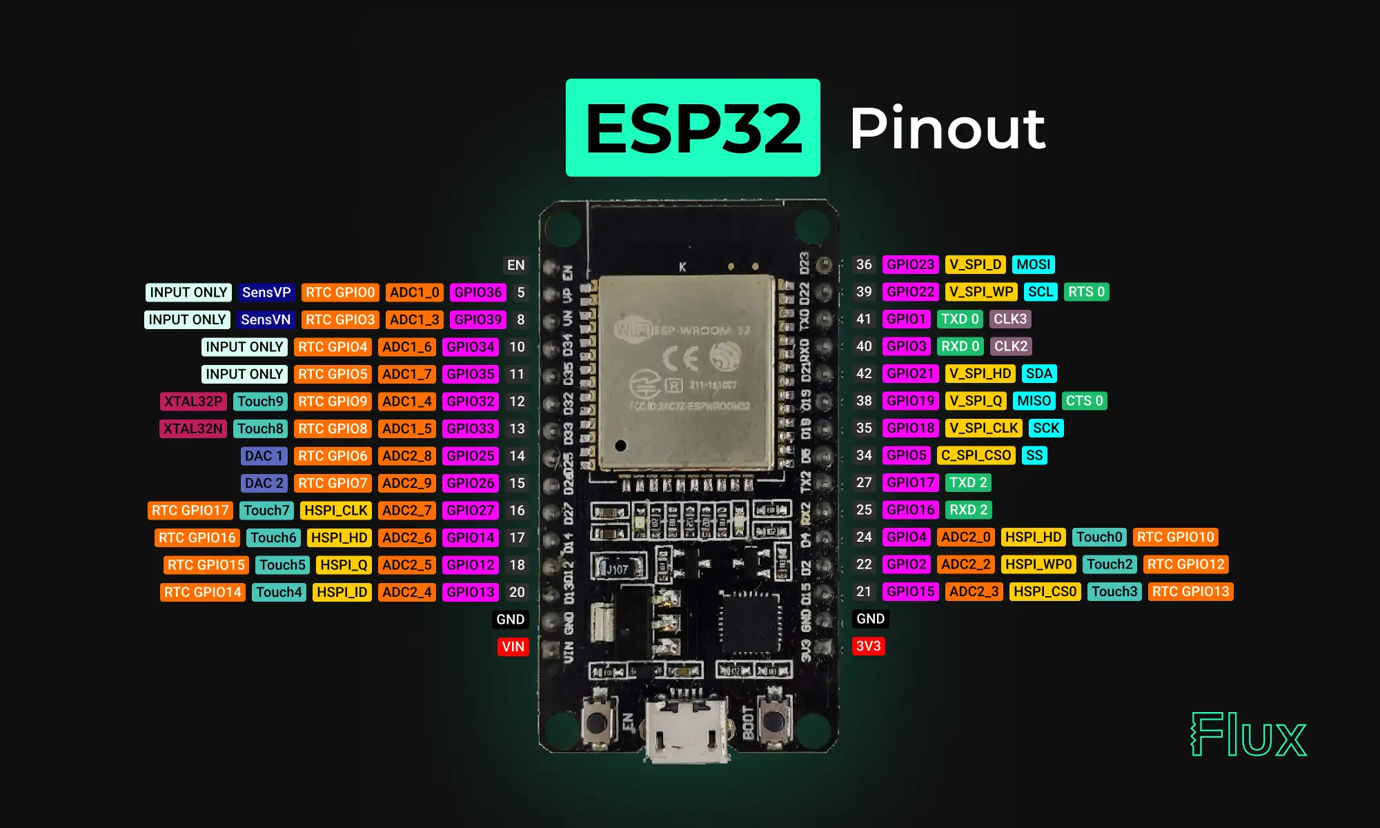
Looking for a comprehensive guide to ESP32 pinout? Check out our article that covers everything you need to know about the ESP32's pins, including digital, analog, PWM, and Strapping pins. Perfect for beginners and experts alike, our guide will help you understand the ESP32's pinout and how to use it in your projects.