April 24, 2025
Guide to GND Fills and Power Planes
Share
BuildWithFlux


That’s where ground planes, zones, and stackup symmetry come in. They’re the quiet guardians of signal integrity, and Flux is built to help you get them right—without the guesswork.
In this post, we’ll explore why these concepts matter, how they impact signal integrity and power distribution, and what to keep in mind as you design. If you want to go deeper into implementation details—like when to use zones, where to place stitching vias, or how to avoid stackup pitfalls—we’ve created a detailed PDF guide just for that.
{{download-gnd-power-guide}}
Every signal you route is part of a circuit. And that circuit includes the return path—the signal that flows back to the source. At high speeds, this return doesn't just wander through your board—it seeks the lowest impedance path back.
That path is normally the ground plane directly beneath the signal layer. If the plane is continuous, the return path stays tight, inductance stays low, and EMI stays minimal.
But if the ground is broken—say, by a split—the return path will form a bigger loop. And bigger loops might mean bigger problems: signal distortion and radiated emissions that could cause a failed EMI test.
Good return paths are invisible when they work, and painfully visible when they don’t.
You’ve probably heard the advice: “Split your ground plane between analog and digital.” Sometimes that’s sound engineering. But often, it leads to more trouble than it solves.
The key question isn’t “Should I split my ground plane?”—it’s “Will this split create more noise than it prevents?”
In most cases, you should avoid splitting the ground plane. Here's why:
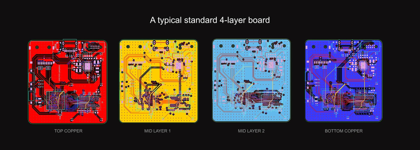
A PCB stackup isn’t just a layer count—it’s a design decision that affects everything from signal integrity to manufacturing yield.
When your layout starts pushing higher speeds or tighter constraints, your stackup becomes critical. It defines the electrical environment for your signals and the mechanical stability of your board.
For most standard boards—say, 4 to 6 layers on 1.6 mm FR4—mechanical issues like warpage are rarely a showstopper with modern fabrication processes. Today’s board houses are well-equipped to handle these with balanced copper and proper lamination.
But in more demanding cases, stack symmetry still matters:
The rule of thumb: the more complex or thermally sensitive your board, the more stack symmetry and copper balance matter. It’s not just about layout—it’s about ensuring the board survives fab, assembly, and real-world use.
If you remember nothing else, start with these rules:
We’ve built these rules into Flux—not as rigid constraints, but as default guardrails. So you can break them when needed—but only when you know you need to.
High-speed, low-noise boards don’t happen by accident. They’re designed intentionally—from the copper up. Whether you're debugging EMI issues or laying out a complex mixed-signal board, your ground strategy is the foundation.
With Flux, you don’t need to memorize every trick in the book. We’ve integrated the most important ones into your workflow—so you can focus on building, not second-guessing.
Ready to ground your designs the right way?→ Open Flux and give your next project the return path it deserves.→ Or dive deeper into Zones and Cutouts » | Stackup Editor »


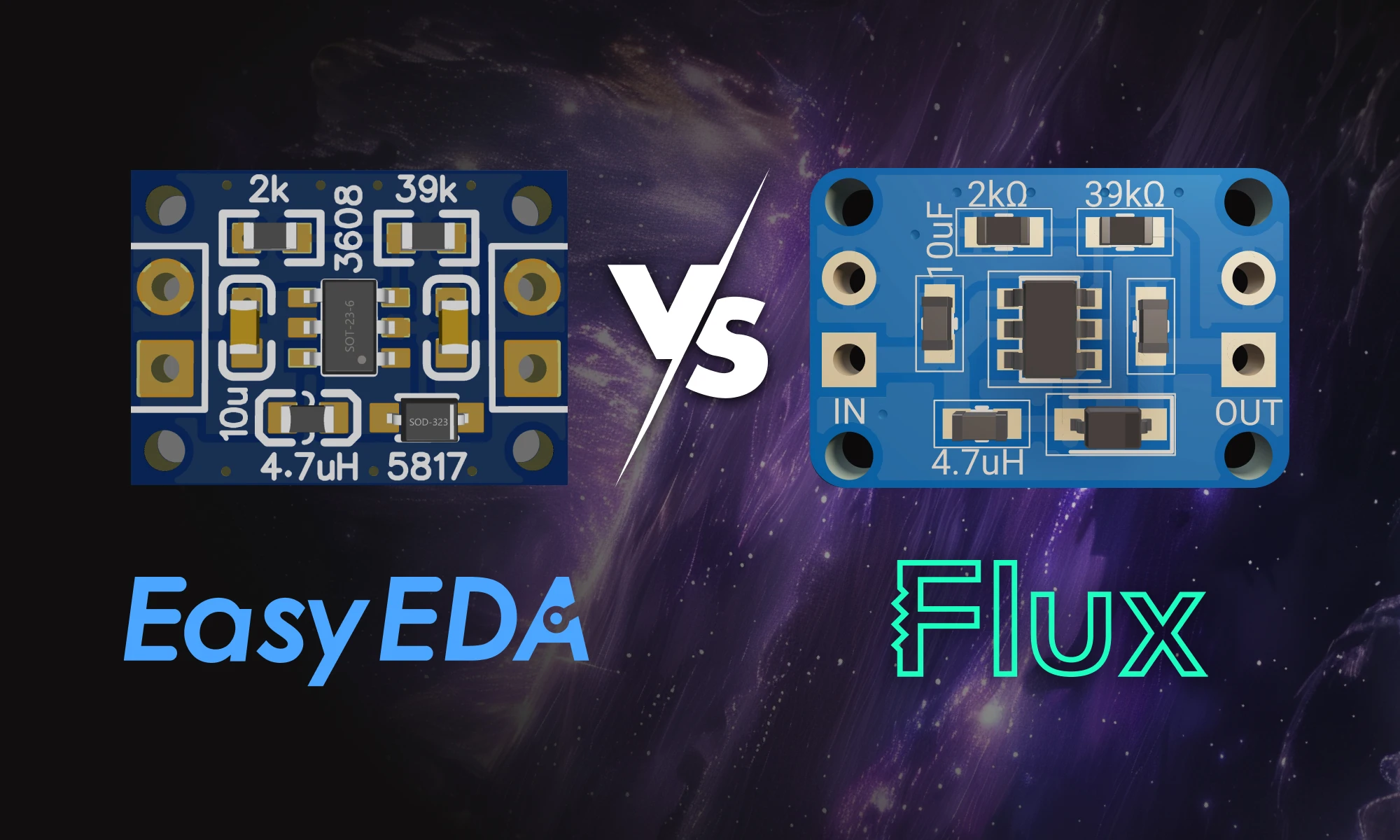
If you’re using EasyEDA and are thinking of making the switch to Flux, learn how the two platforms differ and why Flux might be the next step in elevating your PCB design experience.

The guide provides an easy-to-follow formula for converting mm to mils, essential in engineering and PCB design for precise measurements and applications.


This blog post explores the RS485 communication standard, renowned for its ability to facilitate long-distance, multidrop networking with enhanced noise immunity, making it a preferred choice for industrial settings. Dive into the post to understand RS485's key features and advantages over older protocols.

Designing an AI pin would normally take months, but in this project, we did it in hours. In our step-by-step guide, you'll see how Flux can accelerate your design process and bring your AI pin project to life.

KiCad revolutionized PCB design by making it accessible to everyone. Flux builds on that foundation, offering a browser-based, AI-powered platform that takes your PCB design experience to the next level.

Imagine starting a project with over 800,000+ parts at your fingertips, ready to go without any setup. With Flux community-powered part library, you have everything you need to build at scale —all in one place, with real-time supply chain data, intelligent filters, and powerful AI tools.

Explore more than 20 new Flux Copilot prompts for hardware design. Accelerate brainstorming, component selection, validation and design review to streamline your PCB design.
We’re incredibly excited to announce that we have decided to open up Flux and move out of private beta! What does this mean? If you’re a current user of Flux - nothing will change for you. For new users, this means that we’re now allowing anyone and their team to signup!